INTRODUCTION TO DIGITAL LOGIC GATES
The term LOGIC was used long before Digital Electronics was even thought of. It was used by
philosophers to describe the way in which they determined the meaning of language. Different
descriptions of things were combined using the everyday terms AND, OR and NOT in a very
organised way. This was the basis of LOGIC. In this system each description being considered
could only have one of two states, TRUE or FALSE. The outcome of any combination of TRUE or
FALSE descriptions using AND, OR and NOT were unambiguously defined by this system of LOGIC.
The use of only two states, and the unambiguous outcomes of combinations, was recognised in
the mid 20th Century as being suitable for the design and classification of Digital Electronic
Circuits.
REPRESENTATION OF SIMPLE GATES BY SWITCHES
Consider a circuit with a power supply, a lamp and two switches, A and B. These can be arranged
to form a LOGIC circuit in the following way.
AND Circuit
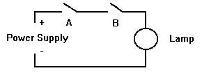
It is clear that for the Lamp to be Lit or ON, then switch A AND switch B need to be ON. This
arrangement is therefore known as an AND circuit. There are four possibilities of switch
settings in the above circuit. A and B OFF, A OFF and B ON, A ON and B OFF and A AND B ON.
This information is usually summarised in a table, known as a TRUTH table, from the original
philosophers usage of TRUE and FALSE for the two states. In Digital Electronics 0 of L is
used for FALSE and 1 or H for TRUE, so the table for an AND circuit looks like this.
             B      A     LAMP

             0      0       0
             0      1       0
             1      0       0
             1      1       1
OR Circuit
The same components of power supply, lamp and switches A and B, can be arranged to form an OR
circuit as follows.
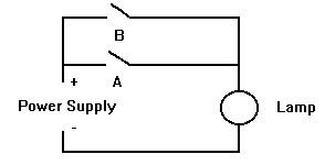
The four possible combinations of switch states are the same as before, but the result is
different. If A and B are both OFF, the lamp is OFF; If A OR B is ON then the lamp is ON.
This can be shown in the following truth table.
             B      A     LAMP

             0      0       0
             0      1       1
             1      0       1
             1      1       1
[ This is actually called an INCLUSIVE OR because it includes the condition A and B ON gives
the lamp ON as well as the A OR B, but it is normally just called an OR circuit.]
NOT Circuit
This is not really suitable for implementing as a switch circuit, but it is the simplest of
the three fundamental gates. It has one input and one output, and simply gives a value on the
output opposite to the on the input. The following truth table summarises this.
                   A     OUTPUT
                   0        1
                   1        0
All other digital logic circuits are made up of these three fundamental forms. In the case of
a top of the range microprocessor, maybe millions of them. We will not be using anywhere near
this number in the circuits to be considered in this course!
PRACTICAL DETAILS OF LOGIC GATES
The circuits shown earlier in switch form are usually implemented using digital electronic
circuits which are now available, built and encapsulated in plastic called Integrated Circuits
or IC's. The term "chip" is often used for the devices known as Integrated Circuits. They are,
of course, made of analogue components, but are considered as "boxes" which produce outputs
for combinations of inputs that can be totally described by the TRUTH table for that type
of circuit. This view of them is reinforced by the use of symbols for the gates which do not
indicate any of the internal workings, or even the power supply connections that they need to
operate! This is to concentrate on the LOGICAL aspect of the circuits. The other information
is given in what are called "pin-outs" or connection diagrams. Here the connections are listed
on a drawing with the number of the pin on the circuit corresponding to it. They are often
drawn on a rectangle in the order in which they appear on the "chip", but this is not really
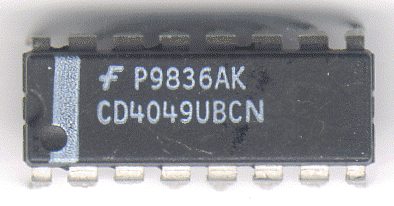
necessary as the pin number is always included. A photograph of a typical IC is shown below.
The number of pins can vary in this type of package, called Dual In Line, or DIL, from 8 to
64. The only way to tell one package from another besides the number of pins, is the
identification numbers and letters printed on them.
Pin 1 of the IC is to the left of the "notch" in the case, often inicated by a "dot" on the
body of the IC. The pin numbers go down one side and up the other as shown in the diagram
below.
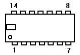
This information will be of use in the practical laboratories which accompany these lectures.
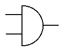
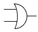
SYMBOLS FOR THE AND, OR & NOT GATE
AND Gate
The output from this gate can be written: y = A.B, where y is the output and the "."
indicates the AND function.
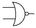
OR Gate
The output from this gate can be written: y = A+B, where y is the output and the "+"
indicates the OR function.
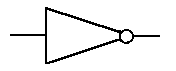
NOT Gate
The output can be called NOT A because it is always the opposite of the
A input. If A was 1, then NOT A will be 0; If A was 0, then NOT A would
be 1. This can be written with a line over the letter, but this is
difficult to produce in word processed documents.
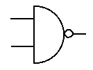
SIMPLE COMBINATIONS TO FORM THE NAND & NOR GATES
Certain combinations of gates occured so regularly in circuits that
engineers thought that a name and special symbol would be useful for
them.
NAND Gate
This was an AND gate followed by a NOT gate, making NOT AND. The
electronics engineers being almost as keen as those in computing on
abbreviations, soon contracted this to NAND. The symbol follows this
contraction.
NOR Gate
In the same way, NOT OR became NOR.
EXCLUSIVE OR CONSTRUCTION
This method of combining gates can be used to make more complex circuits,
and TRUTH tables used to determine what they do.

The above circuit is supposed to implement an EXCLUSIVE OR gate. The
TRUTH table shows how the circuit operation is calculated in sections.
The NOT A and NOT B columns are included to make the calculations easier.
B  NOT B  A  NOT A   X    y  x+y = OUTPUT
0    1    0    1     0    0      0
0    1    1    0     0    1      1
1    0    0    1     1    0      1
1    0    1    0     0    0      0
The output is a 1 only when A or B are different. This is why the circuit
is called an EXCLUSIVE OR because it excludes the case where both
A and B are 1.
Here is an example for next time. Try to draw the circuit for an EXCLUSIVE NOR Gate
Circuit. Not the one for EXCLUSIVE OR followed by an inverter please!!!! Hint: work
out the truth table for a two input circuit as we did above, and then implement it
using gates.
The solution to the above example is shown HERE.