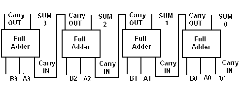
INTRODUCTION TO BINARY ARITHMETIC


Binary arithmetic is the basis of the numerical processing power of digital computer systems. Addition is the foundation of this arithmetic, as to subtract, one of the two numbers is inverted and added; to multiply the number to be multplied is added over and over again and to divide, repeated subtraction is used. The problem of digital binary arithmetic is therefore reduced to designing and building an adder circuit. The first task is to determine what the adder must do.
     Adding two single digits:-

	0+	1+	0+	1+
	0	0	1	1
	-	-	-	-
	0	1	1      10

			       ^
			       CARRY HERE

     This can be summarised in a TRUTH TABLE

		B	A      SUM    CARRY
		0	0	0	0
		0	1	1	0
		1	0	1	0
		1	1	0	1

     Adding three single digits:-

	C	B	A      SUM    CARRY
	0	0	0	0	0
	0	0	1	1	0
	0	1	0	1	0
	0	1	1	0	1
	1	0	0	1	0
	1	0	1	0	1
	1	1	0	0	1
	1	1	1	1	1
     
The TRUTH Tables above provide the basis for the design of the logic circuits required to contruct an Adder circuit.

LOGIC REALISATION OF THE HALF ADDER


The circuit to add two single binary digits is called a HALF ADDER for reasons that will become clearer later. The truth table outcomes provide the basis for the design, by looking at the output column and the inputs which caused it, to find a matching logic function. The TRUTH Table for the HALF ADDER is repeated below. Look at the CARRY column and the A and B columns which produced it.
		B	A      SUM    CARRY
		0	0	0	0
		0	1	1	0
		1	0	1	0
		1	1	0	1
     
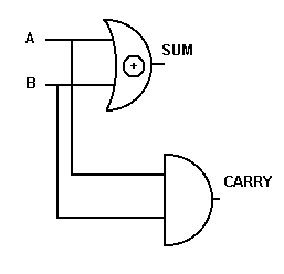
NOTE: CARRY is only 1 when A and B are 1, THEREFORE CARRY is an AND function. The same proceedure can be used with the SUM column. SUM is a 1 only when A and B are different values, THEREFORE SUM is an EXCLUSIVE OR function. The circuit can be drawn from this information, using the EXCLUSIVE OR symbol as one gate rather than the component gates that we know are used in it's construction.

Half Adder Circuit

HALF ADDER circuit

LOGIC REALISATION OF THE FULL ADDER


The process of "inspection", whereby we look at a truth table for the patterns that indicate what functions are involved, is much more complex when the FULL ADDER circuit is being designed. The functions can be seen even here but we are reaching the limits of this technique. The process called KARNAUGH MAPPING, see next week! is one which can help in this sort of design. The TRUTH table for the FULL ADDER is shown below again for reference.
C	B	A      SUM    CARRY
0	0	0	0	0
0	0	1	1	0
0	1	0	1	0
0	1	1	0	1
1	0	0	1	0
1	0	1	0	1
1	1	0	0	1
1	1	1	1	1
       
The SUM column is a 1 when there is an odd number of 1's in the A, B and C column. This suggests EXCLUSIVE OR functions, perhaps (A XOR B) XOR C. The CARRY is rather more complicated, but is a 1 when pairs of A, B andd C are 1. This suggests AND functions OR'd together as in A.B + A.C + B.C. We can use TRUTH tables to see whether the above suggestions are true.
C	B	A      SUM   A XOR B (A XOR B) XOR C
0	0	0	0	0	    0
0	0	1	1	1	    1
0	1	0	1	1	    1
0	1	1	0	0	    0
1	0	0	1	0	    1
1	0	1	0	1	    0
1	1	0	0	1	    0
1	1	1	1	0	    1
      
The above TRUTH TABLE has SUM column and (A XOR B) XOR C column the same proving that SUM can be represented by (A XOR B) XOR C.. The same truth table technique can now be applied to the CARRY column.
C	B	A     CARRY  A.B  A.C  B.C (A.B)+(A.C)+(B.C) 
0	0	0	0     0	   0    0          0
0	0	1	0     0    0    0          0
0	1	0	0     0    0    0          0
0	1	1	1     1    0    0          1
1	0	0	0     0    0    0          0    
1	0	1	1     0    1    0          1
1	1	0	1     0    0    1          1
1	1	1	1     1    1    1          1
      
The above TRUTH TABLE has a CARRY column and (A.B)+(A.C)+(B.C) column the same proving that CARRY can be represented by (A.B)+(A.C)+(B.C). The circuit diagram below is rather different to that suggested by the above logic function, being two cascaded HALF ADDER circuits with their CARRY signals combined in an OR gate. The Truth Tables of the next section will show that they are actually equivalent.

Full Adder Circuit

FULL ADDER circuit

PROOF OF ABOVE CIRCUITS USING BOOLEAN ALGEBRA & TRUTH TABLES


The HALF ADDER circuits were proved in the appropriate section above, but the FULL ADDER circuits have yet to be proved. The SUM circuit can be seen to be two XOR gates, the first is A XOR B and the second is the output from the first, XOR'd with C. This is then (A XOR B) XOR C which we showed was the correct function for SUM. The circuit diagram for the FULL ADDER showed the CARRY to be the output of the CARRY's from both HALF ADDERs.
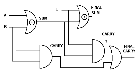
C  B  A CARRY  A XOR B  Y=(A XOR B).C  A.B  (A.B)+Y
0  0  0	  0	  0	      0	        0      0
0  0  1   0       1           0	        0      0
0  1  0	  0	  1	      0         0      0
0  1  1	  1	  0	      0         1      1
1  0  0	  0	  0	      0         0      0
1  0  1	  1	  1	      1         0      1
1  1  0	  1	  1	      1         0      1
1  1  1	  1	  0	      0         1      1
      
The fact that the column for CARRY and the column for (A.B)+Y, which is (A.B)+(A XOR B).C, are identical means that the CARRY produced by the circuit is also correct.

EXTENSION OF ADDER TO ADD MULTI-BIT NUMBERS


Numbers larger than 1 are represented in binary by more than one bit, so any practical adder has to be able to handle multi-bit numbers. The example below is a circuit made up of four full adders connected to add two numbers Bits A0 - A3 and Bits B0 - B3. The results are output as SUM0 - SUM3, with a final CARRY. Each stage, except the first, needs three inputs for A, B and CARRY IN from the previous stage. The first stage needs only two inputs so a half adder could be used there, but for convenience of manufacture all full adders are used. IC's with all four stages on one chip are available implementing the circuit shown below. Note because all stages are full adders, the first stage CARRY IN needs connecting to logic '0'.

Four Bit Adder Circuit

FOUR BIT ADDER circuit


Example for next week, what modifications would have to be made to make a four bit "subtract" circuit?
The solutions to the above examples are shown HERE.